-
Antenna-coupled TES Bolometers used in BICEP2, Keck Array, and SPIDER
The BICEP2, Keck Array, and SPIDER Collaborations, ApJ 812, 176, 2015
| Figures | Download Bundle | ||
|---|---|---|---|
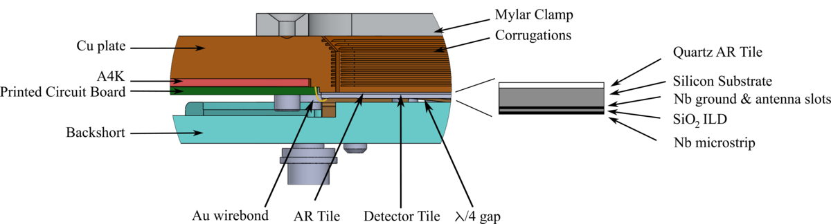
| Focal Plane pictures |

|
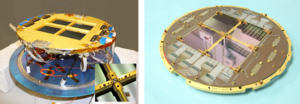
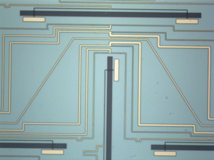
Figure 1: Focal Plane pictures and cross-section. Upper: Top (left) of the BICEP2 focal plane and bottom with backshort removed (right). The arrays of 64 detector pairs per tile are visible at top right. Lower: Major component layers of the focal plane design, with an expanded view of the tile layers at right. Gold wire-bonds thermally sink the tiles to the frame and the frame bears corrugations to suppress coupling to the detectors. Only the detectors at the tile perimeter are at risk of frame coupling. Corrugations are visible in the inset photo in the upper left panel. |
Upper: PDF / PNG Lower: PDF / PNG |
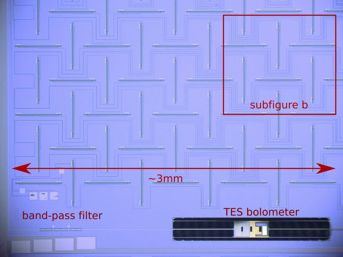
| Major features of the antenna array | 
|
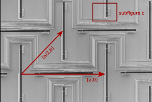
Figure 2: Optical and SEM photographs of major features of the antenna array. Upper: one quarter of a detector element. The antenna array, one filter, and one TES bolometer are visible, as well as DC readout lines for the detector. Middle: SEM micrograph of the slot array (dark rectangles) and oblique Bravais lattice (arrows). The thin white lines comprise the microstrip feed. For 150 GHz detectors, a~600 μm and b=a/2~300 μm; the slot dimensions and spacing in the 95 GHz are 63% larger and those in the 220 GHz detector elements are 47% smaller. Lower: SEM micrograph of microstrip crossover and shunt capacitor at a sub-antenna slot. |
Upper: PDF / PNG Middle: PDF / PNG Lower: PDF / PNG |
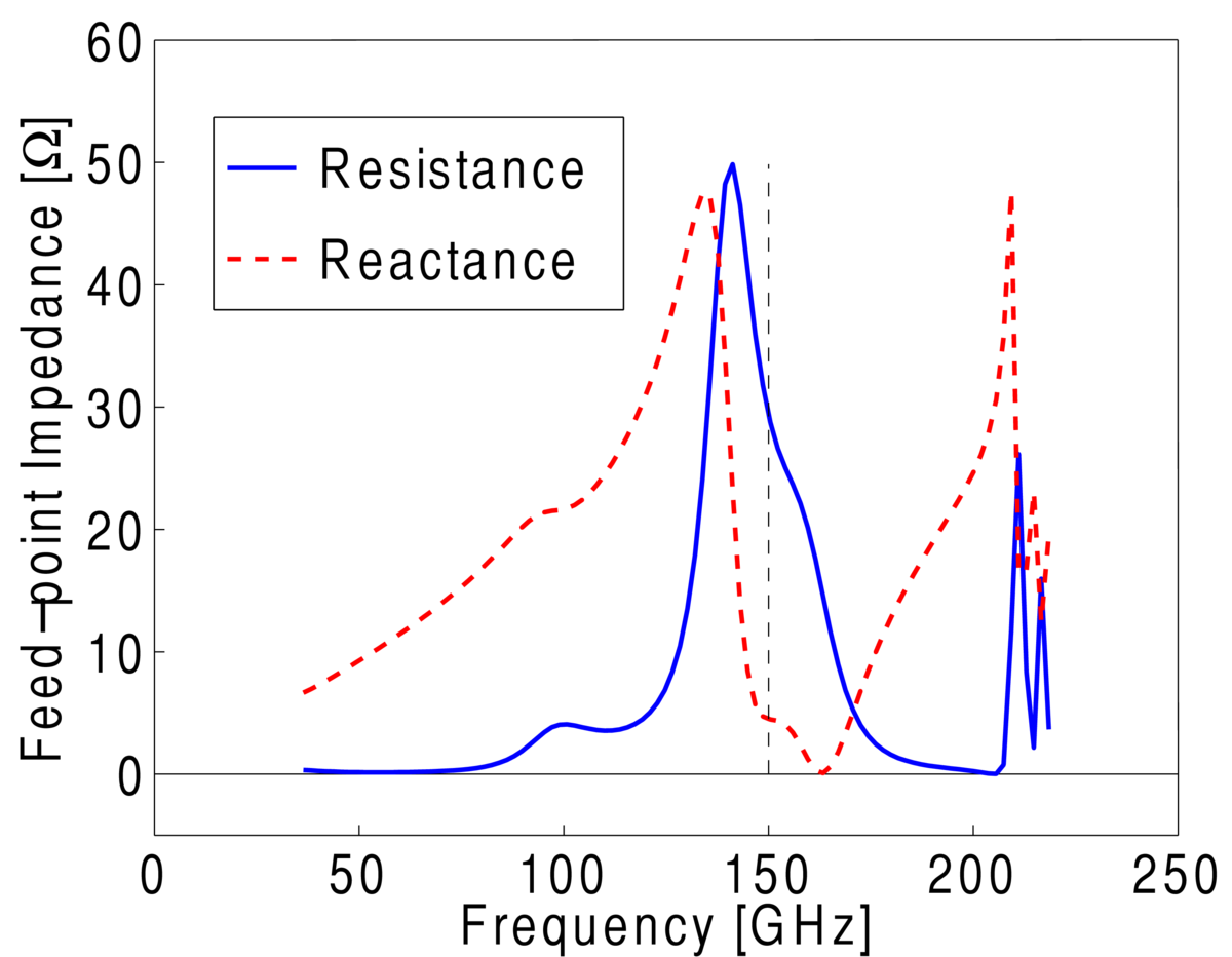
| Simulated feed-point antenna impedance |  |
Figure 3: Simulated feed-point antenna impedance vs. frequency. The dashed vertical line is the band center. | PDF / PNG |
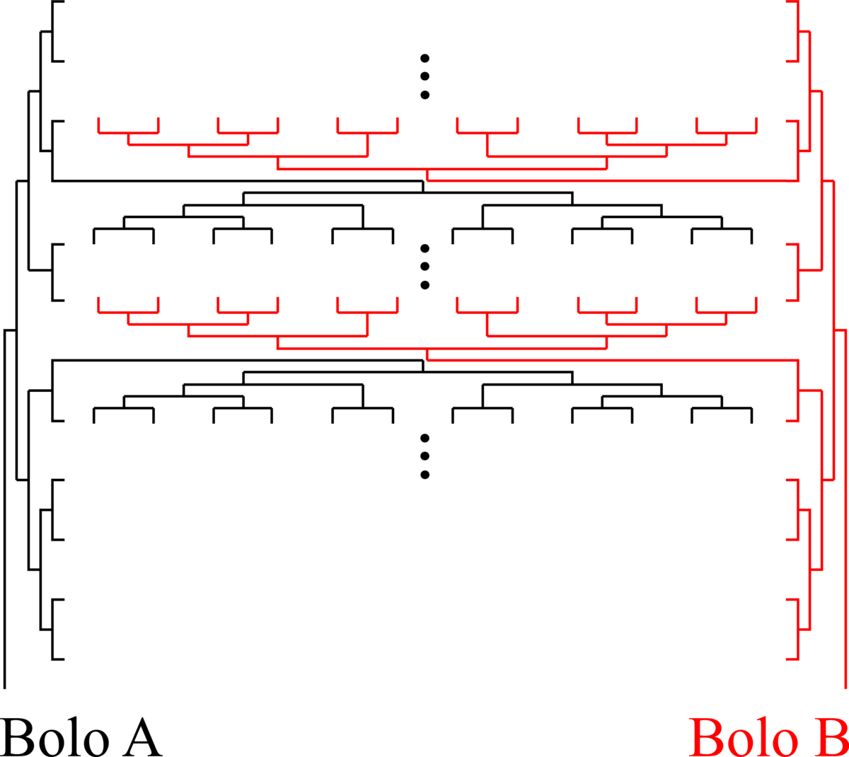
| Feed-network schematic | 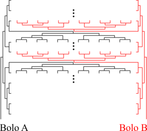 |
Figure 4: Abbreviated feed-network schematic for one detector pair, showing the branch structure for the two polarization summing trees. | PDF / PNG |
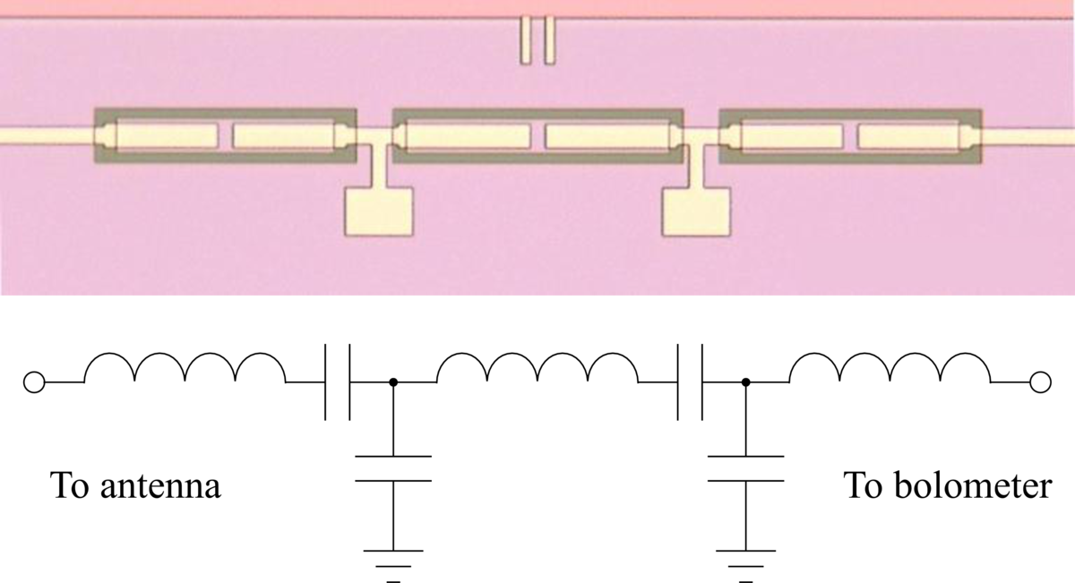
| Filter | 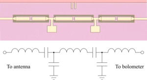 |
Figure 5: Microscope photograph of filter and equivalent circuit for 150 GHz. | PDF / PNG |
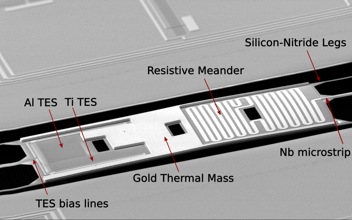
| Released TES bolometer | 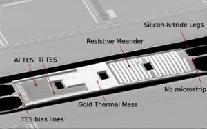 |
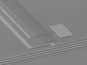
Figure 6: Electron micrograph of a released TES bolometer, illustrating its major components. The gold-meandered microstrip termination is at the right of the photograph and the TESs at left. The thicker gold film in the center of the island ensures thermal stability. | PDF / PNG |
| Cross-section of films in order of fabrication |
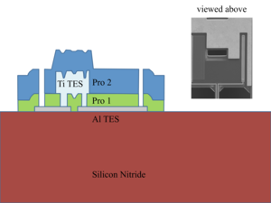
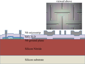
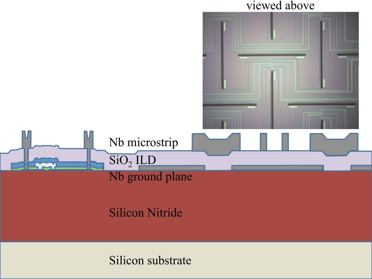
|
Figure 7: Cross-section of films in order of fabrication The aspect ratio between radial and normal dimensions are distorted for clarity. We include photos of how the device looks face-on for reference. Upper: Deposition and etching of films for the TESs and their protect layers. Middle: Deposition and etching of antenna and microstrip features. Lower: Release of TES bolometer. |
Upper: PDF / PNG Middle: PDF / PNG Lower: PDF / PNG |
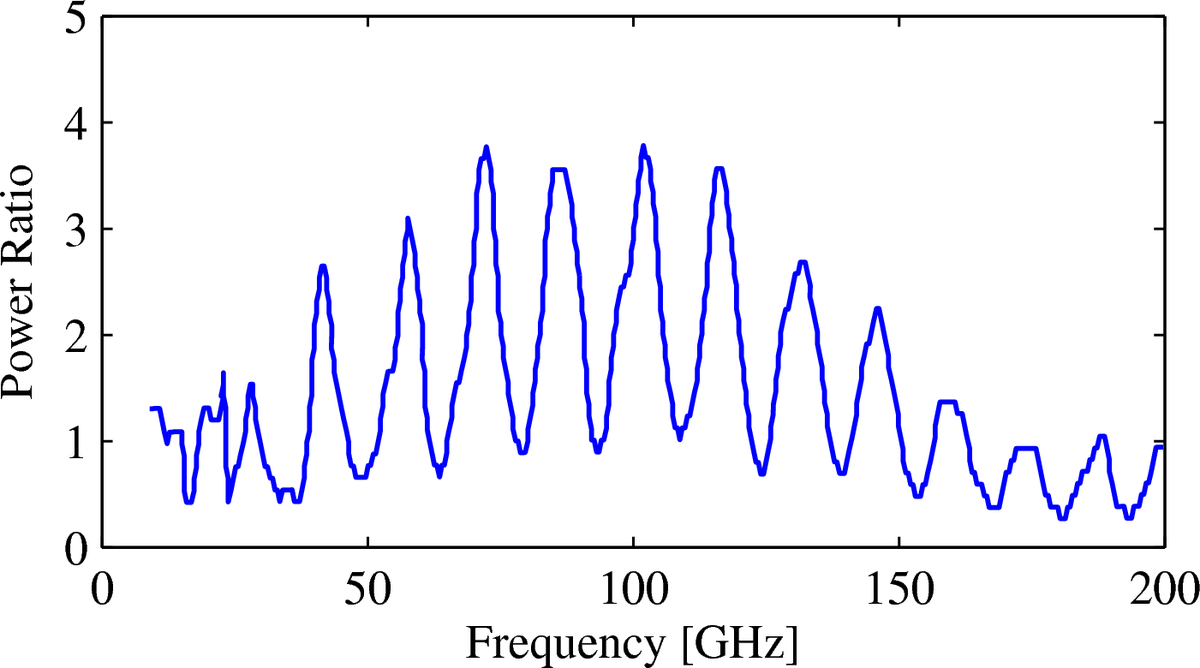
| Wave speed test |


|
Figure 8: Upper: Schematic of a test device for microstrip wave speed, where the mismatched microstrip segment at right forms a Fabrey-Perot cavity. Lower: Standing wave pattern in a device's FTS spectrum. The period is proportional to the transmission line wavespeed. |
Upper: PDF / PNG Lower: PDF / PNG |
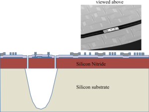
| Microstrip loss test |

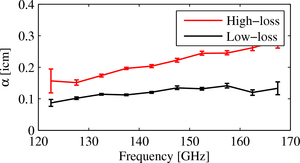
|
Figure 9: Upper: Schematic of a test device for microstrip loss rates, where the DUT is a stretch of transmission line several wavelengths long. Lower: Sample spectra showing power loss per unit length (α = -d [log P]/dx) in films exhibiting low and high loss. Nonlinear increase in loss with frequency has been an indicator of bad process parameters in need of adjustment. |
Upper: PDF / PNG Lower: PDF / PNG |
| Sample far-field detector pattern | 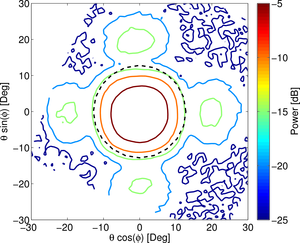 |
Figure 10: Sample far-field detector pattern measured in a test cryostat without an optical stop. Power is normalized to peak on boresight and the dashed line indicates where the f/2.2 camera stop would lie. | PDF / PNG |
| Microstrip layout |
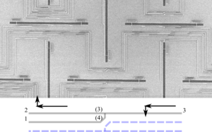
|
Figure 11: Details of microstrip layout in the center of the antenna feed. Upper: Center of the BICEP2-era design. The Cartoon under the picture shows the effective coupler circuit and the ports corresponding to the scattering parameters. The arrows are phasors that illustrate how the intended waves (horizontal) combine with the parasitic coupled waves (vertical). Lower: Modern design with reduced coupling due to greater spaced lines. The extra lengths of line that form compensating phase lags are visible (e.g. bottom of picture), although these are not necessary with the suppressed microstrip coupling. |
Upper: PDF / PNG Lower: PDF / PNG |
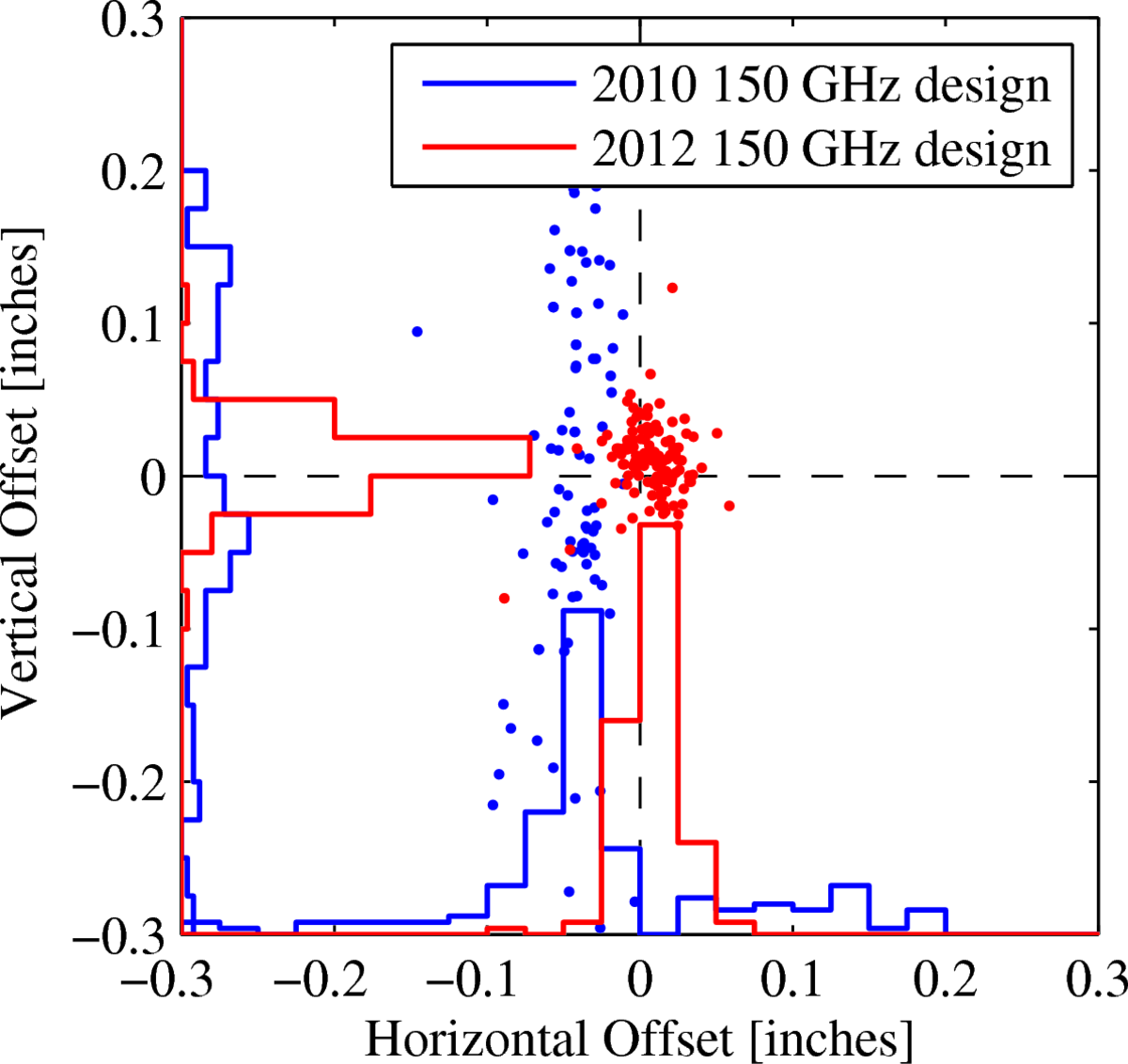
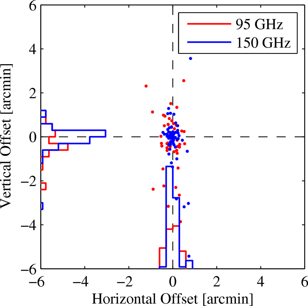
| Beam centroid displacements |
|
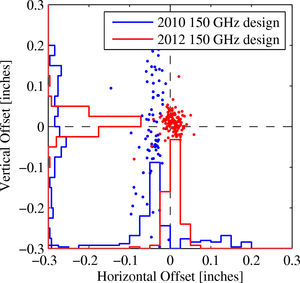
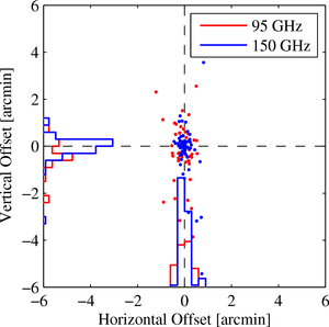
Figure 12: Upper: Beam centroid displacements in the near field before and after fixes were made to the etch recipe. The performance shown in left panel would allow a BICEP1-style pipeline without deprojection to constrain r to 0.1. The deprojection pipeline described in BK-III allows r to be constrained to yet lower levels. Lower: Beam centroid displacements in the far field for two different colors after the recipe was fixed. |
Upper: PDF / PNG Lower: PDF / PNG |
| Thermal conductance | 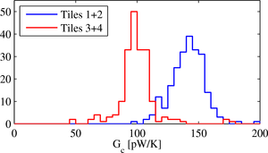 |
Figure 13: Thermal conductance at Tc. This figure demonstrates repeatability within and between tiles. | PDF / PNG |
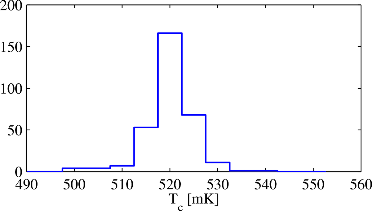
| Titanium TES transition temperature | 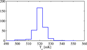 |
Figure 14: Titanium TES transition temperature for four tiles in BICEP2. | PDF / PNG |
| Titanium Normal Resistance | 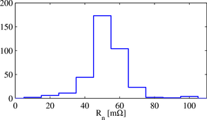 |
Figure 15: Titanium Normal Resistance for four BICEP2 tiles. | PDF / PNG |
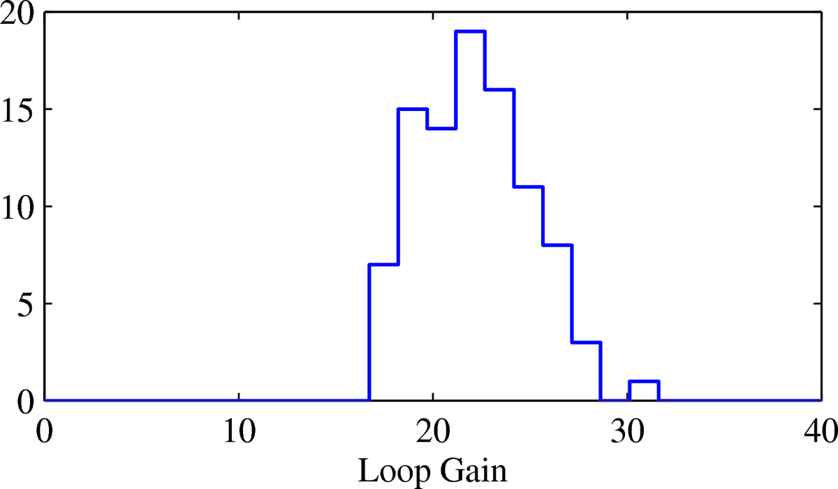
| Time constants and loop gain |
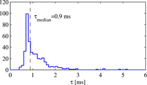

|
Figure 16: Upper: Time constants of BICEP2. These were only carefully measured in transition. Lower: Loop gain of SPIDER. We measured time constant at a variety of biases for SPIDER characterization, allowing a proper measurement of loop gain. Both sets of detectors had similar τ~0.9 ms biased time-constants. |
Upper: PDF / PNG Lower: PDF / PNG |
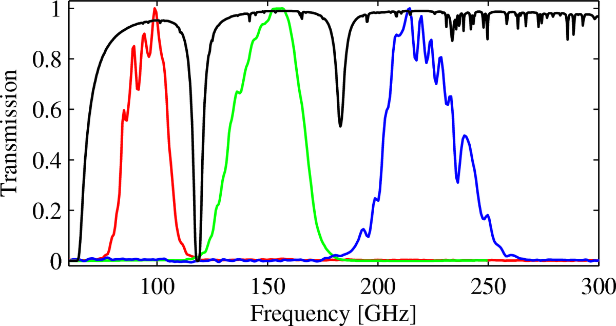
| Measured detector spectra | 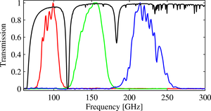 |
Figure 17: Measured detector spectra for devices designed for 95 GHz (red), 150 GHz (green) and 220 GHz (blue). The data for the 150 GHz are from BICEP2, while the others are from a test cryostat. Winter atmospheric transmission at the South Pole is overlaid in black. | PDF / PNG |
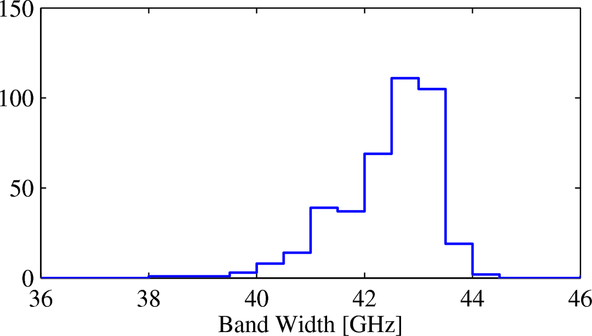
| Spectral response |
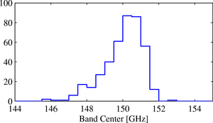
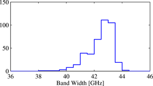
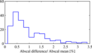
|
Figure 18: Spectral response of detectors in the BICEP2 camera. Upper: histogram of the band centers. Middle: histogram of band widths. Lower: histogram of absolute calibration (abscal) mismatch, where difference and mean are computed between polarization pairs. Calibration is through cross-correlation against Plank 143 GHz. |
Upper: PDF / PNG Middle: PDF / PNG Lower: PDF / PNG |
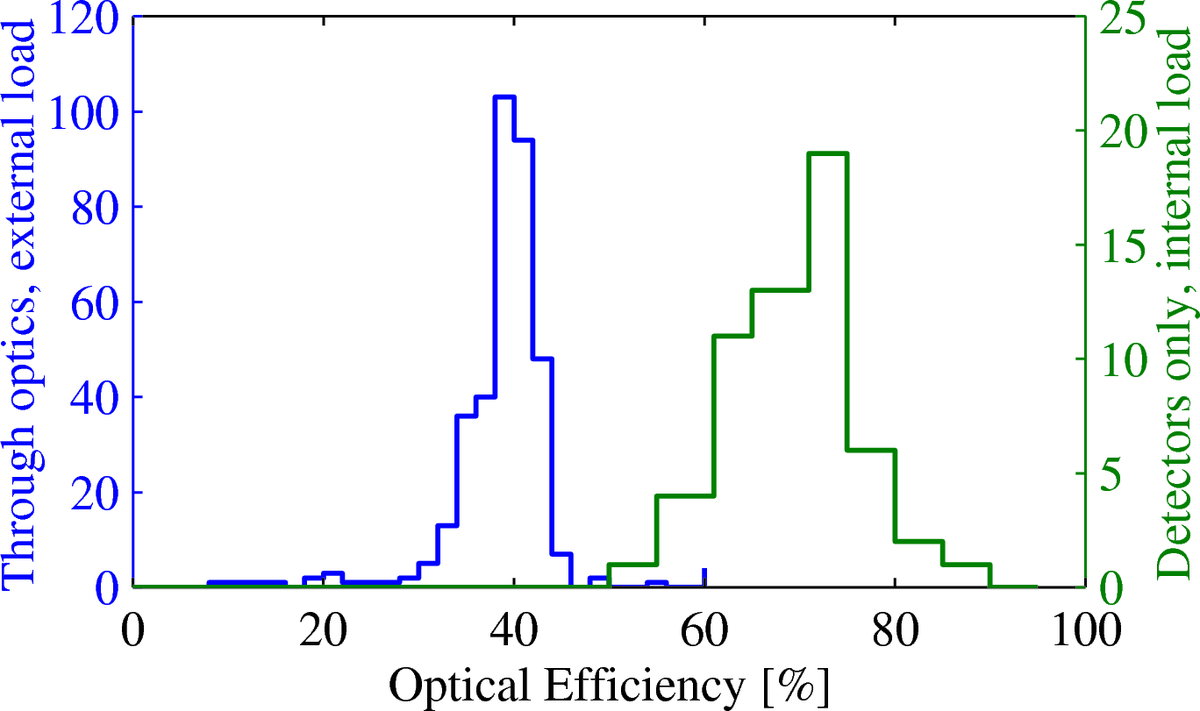
| Optical Efficiencies | 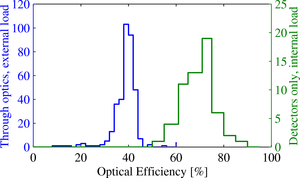 |
Figure 19: Optical Efficiencies of BICEP2 detectors. Blue curves (left-axis) are end-to-end receiver efficiency through all optics; green curves (right-axis) are raw detector efficiencies for a single test-tile from an engineering-grad test focal plane, in response to an internal cold-load. | PDF / PNG |
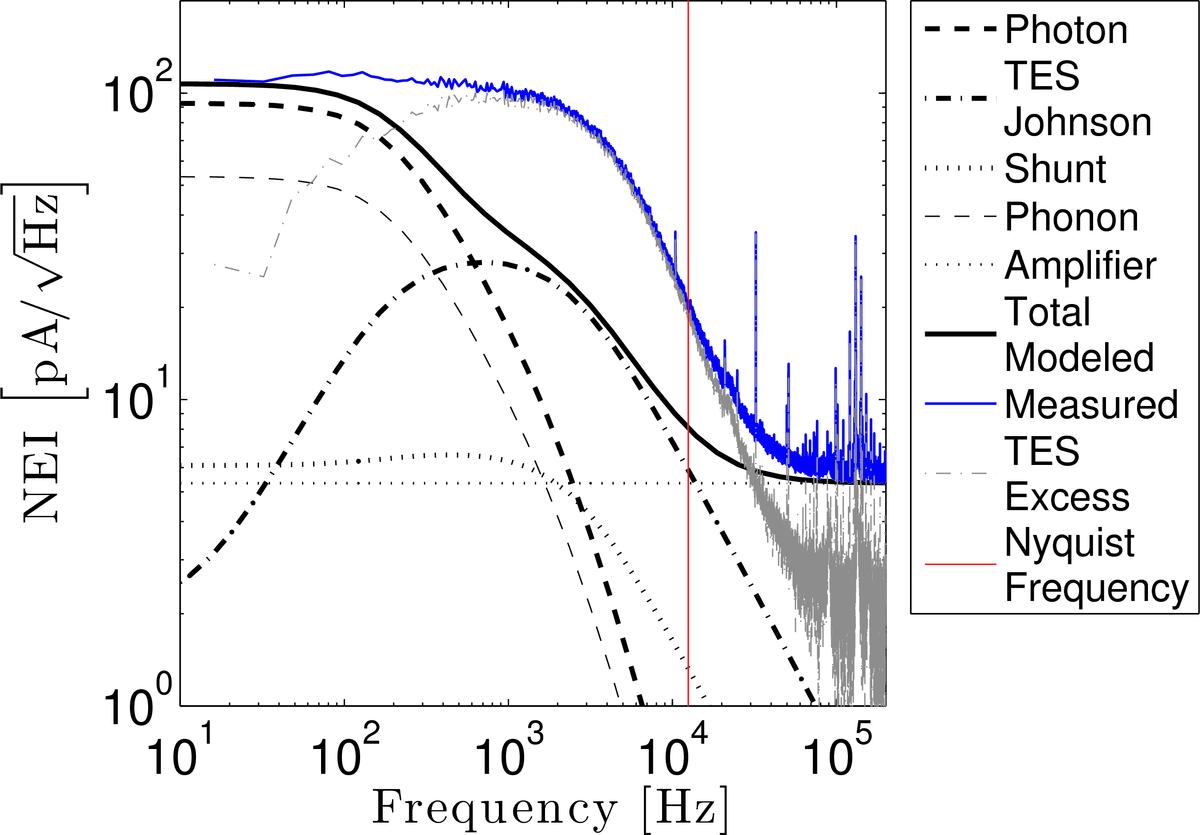
| Single detector noise | 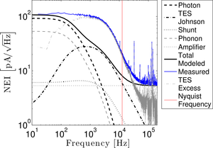 |
Figure 20: Measured and modeled noise for a single detector in the Keck Array. The red line indicates the Nyquist frequency for the multiplexing rate. | PDF / PNG |
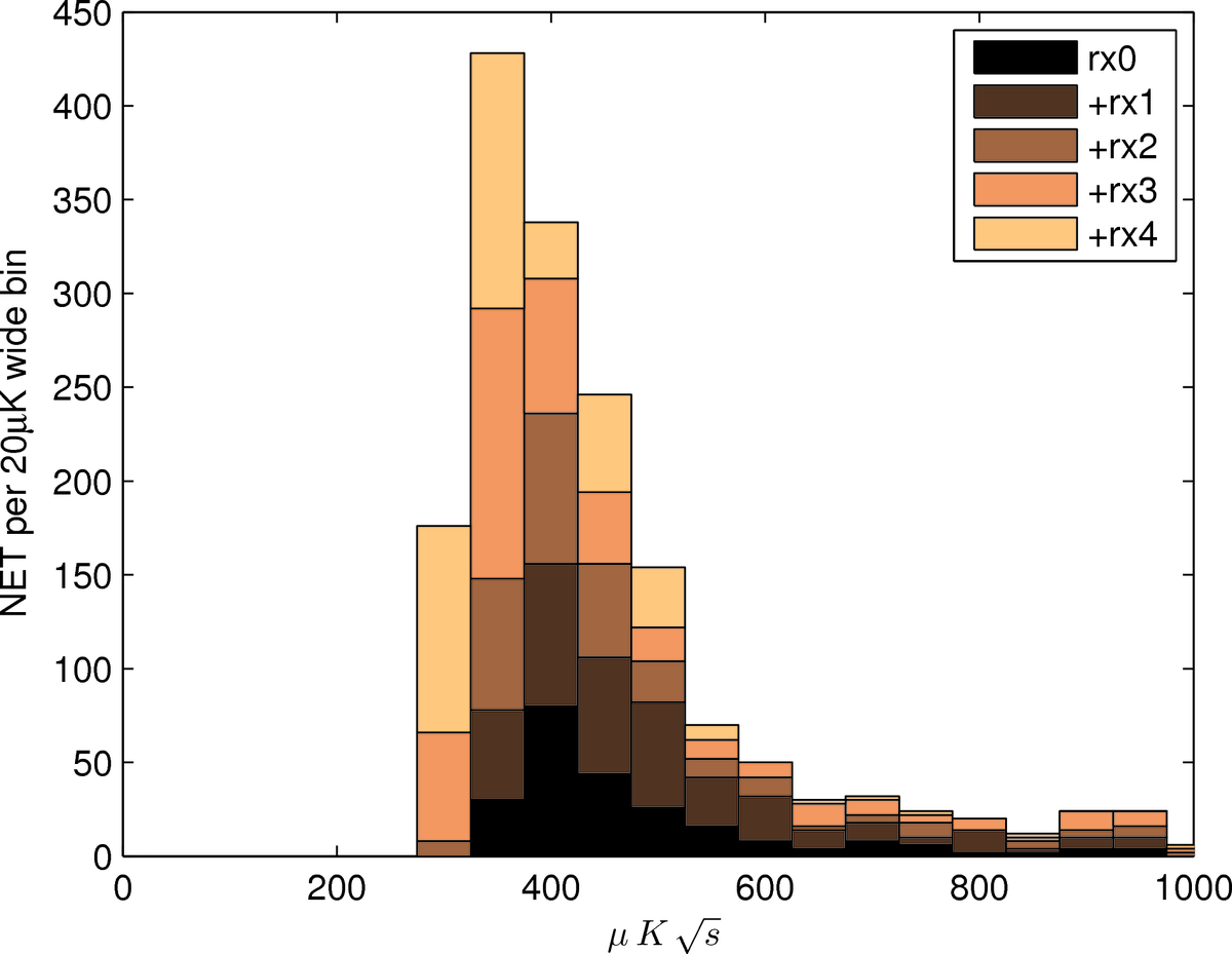
| NET per detector | 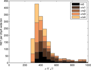 |
Figure 21: NET per detector histogram for the Keck Array in 2013. | PDF / PNG |
History
- 2015-02-02: Posted Antenna-coupled TES Bolometers used in BICEP2, Keck Array, and SPIDER figures.